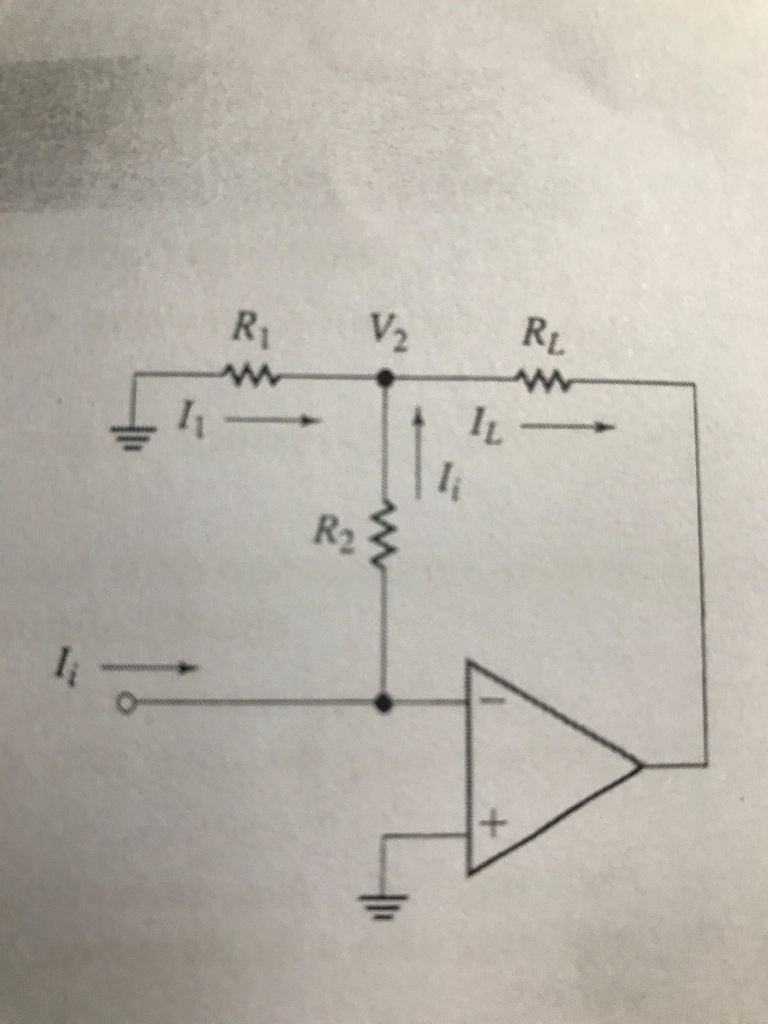
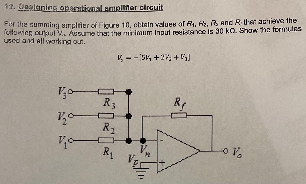
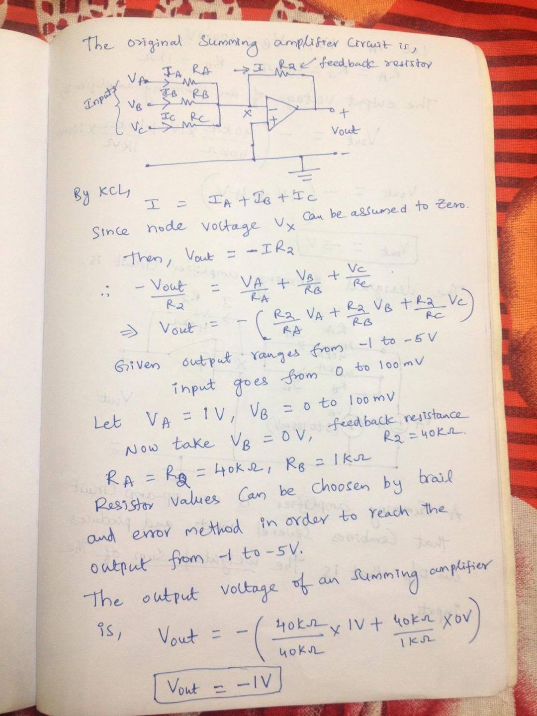
Solved 19 Designing operational amplifier circuit For the Circuit Diagram
Solved 19 Designing operational amplifier circuit For the Circuit Diagram In this chapter we will discuss the basic operation of the op amp, one of the most common linear design building blocks. In section 1 the basic operation of the op amp will be discussed. We will concentrate on the op amp from the black box point of view. There are a good many texts that describe the internal workings of an op amp, so in this An op-amp has two inputs, an inverting terminal (labeled „-") and a non-inverting terminal (labeled „+"). And has a single output. The first input is called inverting because the output voltage is inverse of the voltage applied at the inverting input, times the gain of the amplifier circuit.If we apply the signal to the non-inverting input we get the same signal on the output, times gain. Operational Amplifier Circuits Review: Ideal Op-amp in an open loop configuration Ro Ri + _ Vp Vn Vi + _ AVi + Vo Ip In An ideal op-amp is characterized with infinite open-loop gain A→∞ The other relevant conditions for an ideal op-amp are: 1. Ip =In =0 2. Ri =∞ 3. Ro =0 Ideal op-amp in a negative feedback configuration When an op-amp
the op amp's place in the world of analog electronics. Chapter 2 reviews some basic phys-ics and develops the fundamental circuit equations that are used throughout the book. Similar equations have been developed in other books, but the presentation here empha-sizes material required for speedy op amp design. The ideal op amp equations are devel-

PDF Operational Amplifiers: Basics and Design Aspects Circuit Diagram
Op-amp Basics (part 1): Operational amplifiers (op-amps) are some of the most important, widely used, and versatile circuits in use today. especially with even higher gains. Image 8 shows a circuit design that will allow for a very high input impedance (1MΩ) and high gain (-102), but that can still be built with readily available parts
Offset voltage: The DC voltage that, when applied between the input pins, will cause a DC output voltage of zero. If both inputs were grounded, the output voltage of the op-amp would not be zero. Slew rate: The time taken for the output to change for a given input.Specified as V/mS. Equivalent input noise voltage: The noise performance of the op-amp. An ideal voltage source is placed in series
PDF Op Amps for Everyone Design Guide (Rev. B) Circuit Diagram
Basic OpAmp Design Release 2.0 Oct 20, 2018. Many newcomers into electronics, especially those in the digital world, are often intimidated by opamps (operational amplifiers). They are quite simple but most explanations on how they work confuse the hobbyist. A basic circuit uses two resistors. An input resistor (Rin) and a feedback resistor